It’s coming up on a year since we published our last memory review; possibly the longest hiatus this section of the site has ever seen. To be honest, the reason we’ve refrained from posting much of anything is because things haven’t changed all that much over the last year – barring a necessary shift towards low-voltage oriented ICs (~1.30V to ~1.50V) from the likes of Elpida and PSC. Parts of these types will eventually become the norm as memory controllers based on smaller and smaller process technology, like Intel’s 32nm Gulftown, gain traction in the market.
While voltage requirements have changed for the better, factors relating to important memory timings like CL and tRCD haven’t seen an improvement; we’re almost at the same point we were a year ago. Back then Elpida provided a glimpse of promise with their Hyper-series of ICs. The Hyper part was capable of high-speed, low-latency operation in tandem. Unfortunately, due to problems with long-term reliability, Hyper is now defunct. Corsair and perhaps Mushkin still have enough stock to sell for a while, but once it's gone, that’s it.
The superseding Elpida BBSE variant ICs and a spread of chips from PSC now dominate the memory scene, ranging from mainstream DDR3-1333 speeds all the way to insanely-rated premium DDR3-2500 kits. Some of these parts are capable of keeping up with Hyper when it comes to CL, but do so by adding a few nanoseconds of random access latency due to a looser tRCD. Given that read and write access operations make up a significant portion of memory power consumption, this step backwards in performance may be a requisite factor for reliability – perhaps something was found by Elpida during the production lifetime of Hyper ICs that prompted a re-examination, leading to a more conservative recipe for data transfer/retrieval.
Today’s memory section comeback was fuelled by the arrival of a number of mainstream memory kits at our test labs – many of the kits we were using for motherboard reviews are no longer for sale so we needed to update our inventory of modules anyway. Corsair, Crucial and GSkill kindly sent memory from their mainstream line-ups. The original intent was to look at a few of those kits.
However, during the course of testing these kits, our focus shifted from writing a memory review (showing the same old boring graphs) to compiling something far more meaningful: a guide to memory optimization and addressing, including a detailed look at important memory timings, and an accounting of some of Intel’s lesser-known memory controller features. As such, this article should make a very compelling read for those of you interested in learning more about some of the design and engineering that goes into making memory work, and how a little understanding can go a long way when looking for creative ways to improve memory performance…
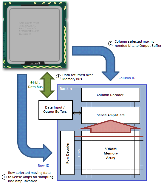
Synchronous dynamic random access memory (SDRAM) is made up of multiple arrays of single-bit storage sites arranged in a two-dimensional lattice structure formed by the intersection of individual rows (Word Lines) and columns (Bit Lines). These grid-like structures, called banks, provide an expandable memory space allowing the host control process and other system components with direct access to main system memory to temporarily write and read data to and from a centralized storage location.
When associated in groups of two (DDR), four (DDR2) or eight (DDR3), these banks form the next higher logical unit, known as a rank. 2GB DDR3 Dual Inline Memory Modules (DIMM) are undoubtedly the most popular density choice among today's enthusiast users. Most new parts of this type are configured as two identical ranks of eight banks each; one side of the DIMM housing those ICs that make up Rank 1, with Rank 2 populating the opposite face of the module. For this reason, single-sided DIMMs typically comprise only a single rank of addressable memory space.
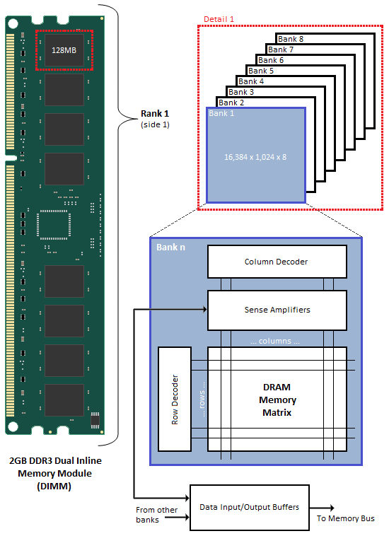
Figure 1 shows the typical functional arrangement of SDRAM memory space. In the case of our example dual-sided dual-rank unbuffered 2GB SDRAM DIMM, the fully populated module contains a total of 16 ICs, eight per side. Each IC contains eight banks of addressable memory space comprising 16K pages and 1K column address starting points with each column storing a single 8-bit word. This brings the total memory space to 128MB (16,384 rows/bank x 1,024 columns addresses/row x 1 byte/column address x 8 stacked banks) per IC. And since there are eight ICs per rank, Rank 1 is 1GB (128MB x 8 contiguous banks) in size, with the same for Rank 2, for a grand total of 2GB per module.
If each row contains 1K (1,024) column address staring points and each column stores 8 bits (1 byte), this would mean each row (page) is 8,192 bits (1,024 x 8 bits) or 1K bytes per bank. It's important to understand that each page of memory is segmented evenly across Bank n of each IC for the associated rank. For this reason, each page is in actuality 8KB (1KB x 8 contiguous banks) in size. So when we talk about IC density we are referring to eight distinct stacked banks and the total memory space therein, whereas when we talk about page space, we are really working with Bank n spread across the total number of ICs per rank. In the end the math comes out the same (8 ICs versus 8 banks), but conceptually it's a critical distinction worth acknowledging if we are to really grasp the ins and outs of memory addressing.
We can now see why the DDR3 core has a 8n-prefetch (where n refers to the number of banks per rank) as every read access to the memory requires a minimum of 64 bits (8 bytes) of data to be transferred. This is because each bank, of which there are eight for DDR3, fetches no less than 8 bits (1 byte) of data per read request - the equivalent of one column's worth of data. Whether or not the system actually makes use of all 8 bytes of transferred data is irrelevant. Any delivered data not actually requested can be safely disregarded as it's just a copy of what is still retained in memory.
SDRAM can, in many ways, be best described as a simple state machine (Figure 2) which is either idle, active, or precharging one or more open banks. As with any machine, transition from one state to another requires a minimum wait time before the system is ready to respond to subsequent requests to do additional work. These delays have a major impact on SDRAM read and write performance, and more importantly, performance of the system as a whole.
Since SDRAM memory cells are really just miniature capacitors, the charge they contain will dissipate away naturally over time due to many factors that can influence the leakage rate, including temperature. A marked reduction in stored charge can result in either data loss or data corruption. In order to prevent this from happening SDRAM must be periodically refreshed by topping off the charge contained in each individual memory cell. The frequency with which this refresh need occur depends on the silicon technology used to manufacture the core memory die and the design of the memory cell itself.
参考https://blog.csdn.net/piscesq329a/article/details/9244723
https://blog.csdn.net/u011240016/article/details/52662193
Reading or writing to a memory cell has the same effect as refreshing the selected cell by issuing a Refresh (REF) command. Unfortunately, not all cells are read from or written to during the normal course of operation and so each cell in the array must be accessed and written back (restored) before the expiration of the refresh interval. In most cases, refresh cycles involve restoring the charge along an entire page. Over the course of the entire interval, every page is accessed and subsequently restored. At the end of the interval, the process begins again. A typical Refresh Period (tREF) is hundreds to possibly a thousand or more clocks.
All banks must be precharged and idle for a minimum of the RAS Precharge (tRP) delay before the Refresh (REF) command can be applied. An address counter, internal to the device, supplies the bank address used during the course of the refresh cycle. When the refresh cycle has completed, all banks are left in the precharged (idle) state. A delay between the REF command and the next Activate (ACT) command or subsequent REF command must be greater than or equal to the Row Refresh Cycle Time (tRFC). In other words, a minimum wait of tRFC cycles is required following a refresh to an idle bank before it can be again activated for access.
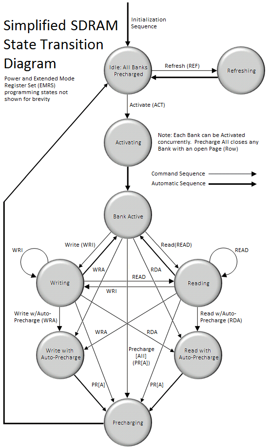
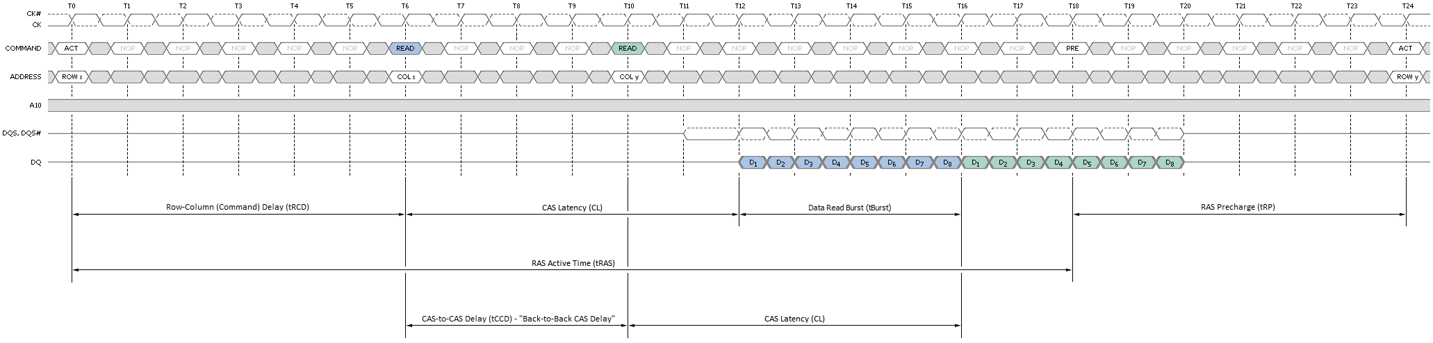
Before the SDRAM is ready to respond to read and write commands, a bank must first be opened (activated). The memory controller accomplishes this by sending the appropriate command (ACT), specifying the rank, bank, and page (row) to be accessed. The time to activate a bank is called the Row-Column (or Command) Delay and is denoted by the symbol tRCD. This variable represents the minimum time needed to latch the command at the command interface, program the control logic, and read the data from the memory array into the Sense Amplifiers in preparation for column-level access.
Following activation, the open bank contains within the array of Sense Amps a complete page of memory only 8KB in length. At this time, multiple Read (READ) and Write (WRI) commands can be issued, specifying the starting column address to be accessed. The time to read a byte of data from the open page is called the Column Address Strobe (CAS) Latency and is denoted by the symbol CL or tCAS. This variable represents the minimum time needed to latch the command at the command interface, program the control logic, gate the requested data from the Sense Amps into the Input/Output (I/O) Buffers, through a process known as pre-fetching, and place the first word of data on the Memory Bus.
Only one page per bank may be open at a time. Access to other pages in the same bank demands the open page first be closed. As long as the page remains open the memory controller can issue any combination of READ or WRI commands, sometimes switching back and forth between the two, until such time as the open page is no longer needed or a pending request to read/write data from an alternate page in the same bank requires the current page be closed so that another may be accessed. This is done by either issuing a Precharge (PR) command to close the specified bank only or a Precharge All (PRA) command to close all open banks in the rank.
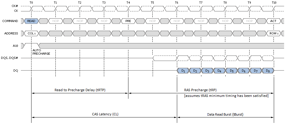
Alternatively, the Precharge command can be effectively combined with the last read or write operation to the open bank by sending a Read with Auto-Precharge (RDA) or Write with Auto-Precharge (WRA) command in place of the final READ or WRI command. This allows the SDRAM control logic to automatically close the open page as soon as certain conditions have been met: (1) A minimum of RAS Activation Time (tRAS) has elapsed since the ACT command was issued, and (2) a minimum of Read to Precharge Delay (tRTP) has elapse since the most recent READ command was issued.
Precharging prepares the data lines and sense circuitry to transmit the stored charge in the Sense Amps back into the open page of individual memory cells, undoing the previous destructive read, making the DRAM core ready to sample the next page of memory to be accessed. The time to Precharge an open bank is called the Row Access Strobe (RAS) Precharge Delay and is denoted by the symbol tRP. The minimum time interval between successive ACT commands to the same bank is determined by the Row Cycle Time of the device, tRC, found by simply summing tRAS and tRP (to be defined). The minimum time interval between ACT commands to different banks is the Read-to-Read Delay (tRRD).
The process of moving data in and out of the Memory Array and over the Memory Bus is not overly complicated, although the massive parallelization of the actual effort can make it somewhat difficult to fully envision what's really happening without some pretty concise visual aids. We'll try our best to help you out in this regard.
Both read and write access to DDR[3] SDRAM is burst oriented; access starts at a selected location and continues in a pre-programmed sequence for a Burst Length (BL) of 8-bits, or 1 byte, per bank. This begins with the registration of an ACT command and is followed by one or more READ or WRI commands.
Chip Select (S0#, S1#), one for each rank, either enables (LOW) or disables (HIGH) the command decoder which works like a mask to ensure commands are acted upon by the desired rank only.
The length of the each Read Burst (tBurst) is always 4 clocks (4T) as DDR memory transmits data at twice the host clock rate (4 clocks x 2 transactions/clock = 8 transactions or 8 bits per bank).
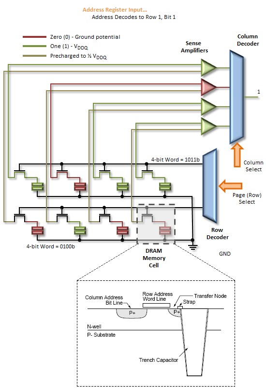
The address bits registered coincident with the ACT command are used to select the bank and page (row) to be accessed. For our hypothetical 2GB DIMM described on Page 2 of this article, Bank Selects BA0-BA2 indicate the bank and Address Input Selects A0-A13 indicate the page. Three bits are needed to uniquely address all eight banks; likewise 14 bits are needed to address all 16,384 (214) pages.
The address bits registered coincident with the READ or WRI command are used to select the targeted starting column for the burst. A0-A09 select the column starting address (210 = 1,024). A12 is also sampled during this operation to determine if a Burst Chop (BC) of 4-bits has been commanded (A12 HIGH). Even though a Burst Chop delivers only half that data of a regular Read Burst, the time period to complete the transfer is still the same: 4T. The SDRAM core simply masks the outgoing data clock strobe for the second half of the full read cycle.
During a Precharge command A10 is sampled to determine whether the precharge is intended for one bank (A10 LOW; BA selects) or all banks (A10 HIGH).
Data Input/Output pins DQ0-DQ63 provide the 64-bit wide data interface between the memory controller embedded in the CPU and each DIMM. Those with a triple-channel capable CPU, like the Intel Core i7-series processor, will come to understand why the memory bus width is reported as 192-bit – three independently operated channels each with a 64-bit interface makes 192. Those of you running a Core 2 or a Core i3/i5 will have to make do with just two channels for a total bus width of 128 bits.
Each channel can be populated with up to two DIMMs. This means there could be a maximum of four ranks per channel, assuming we install a matched pair of dual-rank modules. Installing more than one DIMM per channel does not double the Memory Bus bandwidth, as modules co-located in the same channel must compete for access to a shared 64-bit sub-bus; however, adding more modules does have the added benefit of doubling the number of pages that may be open concurrently (twice the ranks for twice the fun!).
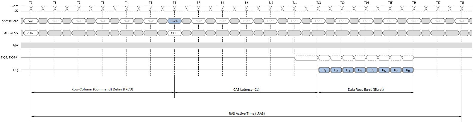
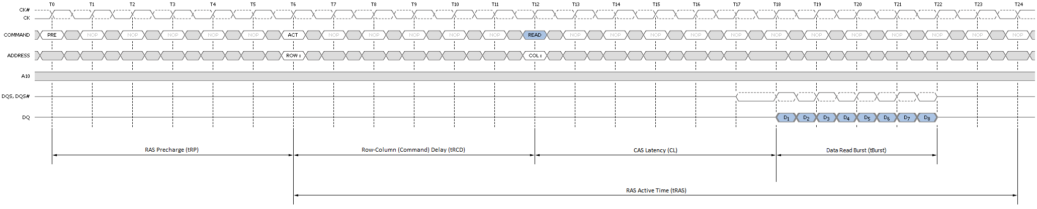
Figure 3 attempts to provide a top-down look at the minimum cycle needed to first open a page in memory, and then read data from the activated page; Figure 4 shows the same, only from a much more fundamental perspective; and Figure 5 provides a detailed accounting of the timing involved.
In this example we assume the bank has no open page, thus is already in the proper precharged state to support a new page access command. Step 1 selects the bank; Step 2 selects the column; and Step 3 bursts the data out over the Memory Bus. A 1-bit row address and a 2-bit column address are all we need to read any data stored in our 2 x 4-bit x 1 (bank) Memory Array.
An Activate command prompts the routing of the specified page address to be accessed to the Row Decoder where it triggers the chosen Word Line to appear at the input of the Sense Amps. As previously stated, this takes a finite time - Row-Column (or Command) Delay (tRCD) is used to program the minimum wait time the memory controller allows for this to occur before it issues the next command in the sequence. Attempting to set too low a timing can lead to inconclusive operation, often resulting in data corruption and other data access issues that ultimately lead to system crashes and other application errors.
Next, the column address provided with the Read command selects the right Bit Line, beginning the process of disregarding those bits that were not addressed. The wait associated with these events is the CAS Latency (CL or tCAS).
The Sense Amps work by sensing the direction of the voltage swing induced on the sense line when the Word Line is activated. Activating the page gates-on the switching element holding back the accumulated charge in a trench filled with dielectric material used to create the capacitive storage element of the memory cell. When this happens the sense line, starting from VRefDQ (½ VDDQ), either swings positive or negative, depending on the potential of the sampled memory cell. An increase in voltage encodes a 1, while a decrease means 0.
The Sense Amps are not comparators. Rather, each Sense Amp interfaces with a pair of memory cells, reducing the total number of amplifiers needed to otherwise sense the entire array by a factor of two.
Following the read, any charge stored in the memory cells is obliterated. This is what is meant by a destructive read: not only do the Sense Amps cache the page for access, they now hold the only known copy of that page of memory! Precharging the bank will force the Sense Amps to "write" the page back to the array and will prepare the sense lines for the next page access by "precharging" them to ½ VDDQ. This accomplishes two thing: (1) It returns all sense rails to a known, consistent potential, and (2) it sets the pre-sense line voltage at exactly half the full-scale value of VDDQ, ensuring whatever the potential stored in the cell, there will be a swing in voltage when the proper Word Line is activated.
Every read/write memory transaction can be segmented by type into one of three performance bins depending on the status of the bank/page to be accessed. These bins, in order of best to worst, are page-hit, page-empty, and page-miss. For the most part, anything we can do to increase the number of page-hit transactions or reduce the number of page-miss transactions is a good thing.
A page-hit access is defined as any read or write operation to an open page. That is, the bank containing the open page is already active and is immediately ready to service requests. Because the target page is already open, the nominal access latency for any memory transaction falling into this category is approximately tCAS (the CAS Latency of the device).
Click to enlarge
Figure 6 shows the minimum read latency associated with a best-case page-hit scenario. For a part with a CAS Latency of 6T, the memory controller waits only six short clocks before the start of data return. During a Read with Auto-Precharge, the Read command will execute as normal except the active bank will begin precharging CAS-latency (CL) clock cycles before the end of the burst. This feature allows the precharge operation to be partially or completely hidden during periods of burst read cycles, dependent on CL. When tuning our systems we always seek to set tRTP such that tRTP + tRP equals CL + tBurst for exactly this reason. Put another way, if CL and tRP are the same set 4T for DDR3 (2T for DD2).
Sequential reads to the same page make these types of transactions even more profitable as each successive access can be scheduled at a minimum of tBurst (4T) clocks from the last. The timing is captured as the CAS-to-CAS Delay (tCCD) and is commonly referred to as 'Back-to-Back CAS Delay' (B2B), as shown per Figure 7. This feature makes possible extremely high data transfer rates for total burst lengths of one page or less - in our case, 8KB.

Click to enlarge
Although not ideal, a page-empty access is still preferred to a miss. In this case the bank to be accessed is Idle with no page open. Common sense tells us any attempt to read or write data to a page in this bank first requires we Activate the bank. In other words, nominal access latency now includes the time to open the page - Row-Column (or Command) Delay (tRCD). This is a doubling of the minimum access latency when compared to that of the page-hit case! Twelve cycles (tRCD + CL) now elapse before the first word is returned. Figure 8 shows this the detail.
Click to enlarge
Finally, as if the relative penalty of page-empty access wasn't bad enough, here comes page-miss. A miss occurs anytime a memory transaction must first close an open page in order to open an alternate page in the same bank. Only then can the specified data access take place. First closing an open page requires a Precharge, adding the RAS Precharge (tRP) delay to any already lengthy operation. As you can see by Figure 9, the nominal latency of an access of this type is three times that of one page-hit operation!
Click to enlarge
The relative gain/loss ratio for each access type can be quickly assessed simply through a cursory review of the most basic device timings. Imagine a memory kit rated for operation at DDR3-1600, 6-6-6-18 (CL-tRCD-tRP-tRAS): With nothing more we can estimate six cycles for a page-hit access, 12 cycles for a page-empty access, and 18 cycles for a page-miss access.
Normalized to the page-hit access latency, page-empty access is twice as long, and page-miss access is a whole three times as long. If we combine this with what we know about the inner functions of the SDRAM state machine we see page-hit and page-miss are really just subsets of the same bank state (active). Of course, page-empty access necessarily implies an idle bank. The following proof rewards us with some powerful insight.
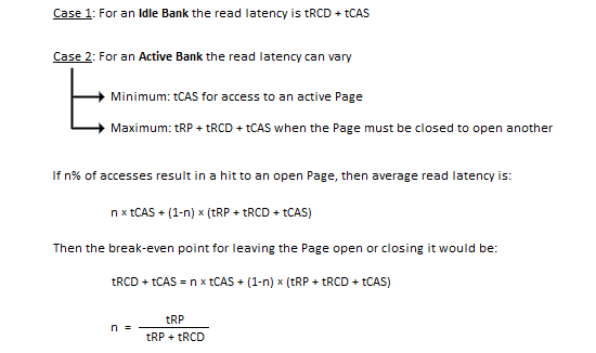
The variable n also represents the percentage of accesses to banks with open pages that must result in a page-hit access if we are to simply pace the nominal access latency that would be achieved if every read access was to an idle bank. And the only thing this depends on is the RAS Precharge delay and the Row-Column (or Command) Delay of the device in question.
You would think by working to maximize n, performance would be maximized as well. And you'd be right. Let's take what we've learned thus far and step it up a notch. We promise, after this you'll never see memory timings in the same light ever again.
Before proceeding, we've prepared a video for those of you that would like to view a few simple animations meant to help visualize each transaction type:
What do you mean you've never heard of Adaptive Page Management (APM) Technology? Well, that must be because Intel Marketing doesn't seem to feel the need to bring it up.
Simply put, Intel's APM determines, based on the potential implications of pending memory transactions, whether closing open pages, or allowing them to remain open longer may be beneficial to overall memory performance. In response, the memory controller may (or may not) elect to issue commands to close pages, depending on the programmed operation.
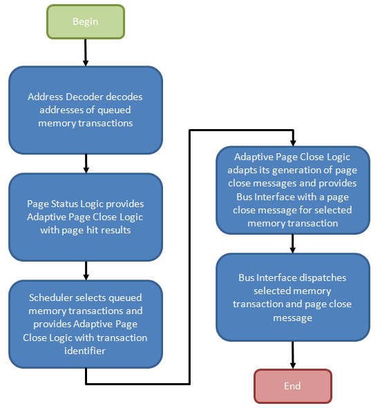
Figure 10 provides the general flow of events required to manage such a process. In our explanation we intend to introduce you to all known register settings needed to adjust the functional control policy, but first we need to detail the necessary actions, and purpose, of the design elements that make up such a mechanism. A better understanding of the underlying logic will pay dividends as you attempt to dial in measurable performance improvements through experimentation.
Per Figure 11, the Transaction Queue stores memory transactions generated by the processor. Unlike a typical First-In-First-Out (FIFO) queue with a tail, into which memory transaction may be pushed, and a head, from which memory transactions may be popped, this transaction queue is a plurality of storage elements allowing single memory transactions to be removed from the list and dispatched toward the memory in a different ordering than when originally added to the queue.
Command re-ordering can improve perceived memory performance by grouping together reads/writes to a common physical page in memory, saving the time that would otherwise be needed to later re-open the same page, should a concurrent access to the same bank force it to close early. After all, the minimum delay between sequential accesses to the same open page is equal to the CAS Latency (CL or tCAS) of the device. Accessing a bank (opening a page) increases the latency of the post-interleaved operation by the Row-Column (or Command) Delay (tRCD), approximately doubling the effective data access time.
One should also appreciate that there are varying degrees of freedom when shuffling transactions in time. Like in the case of a read and write to the same memory location: the memory controller would be disallowed from moving the dependent read either ahead of or behind the associated write as the ordering must be implicitly maintained or coherency will be lost.
The Address Decoder partially decodes the memory transactions stored in the Transaction Queue as needed to determine the bank and page selected by each queued request. From there, the Bank Select messages control the multiplexers used to input the contents of a Bank Register to a comparator used to check if the selected page was also the most recently opened page for that bank (as such, each Bank Register is large enough to store n bits where each bank comprises 2n pages). A match results in the creation of a Page-Hit Result message.
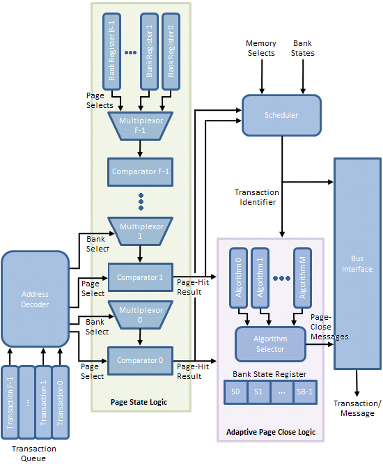
Triggered by the Page State Logic, the Scheduler fetches pre-identified queued memory transactions for re-ordering based on the Memory Selects (both bank and page) and the associated Page-Hit Results. An array of Bank State Registers track actions performed upon each bank by storing a state-word indicating, among other things, whether the Adaptive Page Close Logic decided to close the bank in response to a previous memory transaction to the same bank.
Finally, based on the policy instantiated by the Algorithm Selector, a Page-Close Message either is or is not generated based on the same Page-Hit Results, Bank State Registers, and Bank/Page Selects in an effort to increase the number of subsequent page-hit accesses and/or decrease the number of page-miss accesses.
An immediate and tangible gain is achieved for every successfully re-ordered transaction as a page-hit access is more efficient than a page-empty, or at worst, a page-miss. This is always the case with Core i7 and is one of this architecture's well known shinning points. Switch off Adaptive Page Management (disable Adaptive Page Closing in BIOS) and this is where the process ends. The page may stay open for some finite time or it may be closed right away; we're not sure as there's really no way to know without some inside help.
The Adaptive Page Close Logic must now decide whether to collect all winnings, and close the page, or let it ride, and leave it open just a while longer. While another page-hit access may yield further gains, "guessing" wrong will cause a costly page-miss access in place what would have been just a page-empty access. If only there were some way the system could measure the effectiveness of previous close decisions and then adjust policy to fit...
Surprise! The Page Manager - made up of the Page State Logic, Adaptive Page Close Logic, and Scheduler - does exactly this. How this effectiveness is measured, and how the result of that evaluation is used to adapt the decision-making process is our next topic of discussion.
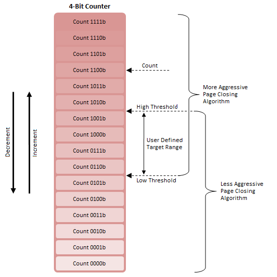
First, consider a 4-bit counter with two adjustable thresholds (Figure 12). When Count is greater than High Threshold, Algorithm A is deemed appropriate; the same is true concerning Algorithm B and Count less than Low Threshold.
For the range between High Threshold and Low Threshold, either algorithm may be in effect. This is because a switch from Algorithm B to Algorithm A will occur only with Count greater than High Threshold and increasing and a switch from Algorithm A to Algorithm B will occur only with Count less than Low Threshold and decreasing.
The overlap range is also the Target Range as the system will naturally attempt to maintain Counter between these two points. This is true since Algorithm A tends to lower Count while Algorithm B tends to raise Count. This system acts to reduce or eliminate rapid thrashing between algorithms.
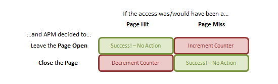
Next, define a truth table (Figure 13) defining how Count will vary. By doing so we can encode a feedback mechanism into our system. Successful predictions by the Adaptive Page Close Logic - a prevented page-miss access (good) in response to a decision to close a page or a facilitated page-hit access (good) in response to a decision to leave a page open - suggest no change to policy is required and so never modify Count.
For a facilitated page-miss access (bad) due to a poor decision to leave a page open, increment Count. If Count were to trend upward we could conceivably conclude that the current policy was most often wrong and not only that, tended to leave pages open far too long while "fishing" for page-hit operations. The current algorithm must not be closing pages aggressively enough.
For a prevented page-hit access (bad) due to a poor decision to close a page early, decrement Count. If Count were to trend downward we would suspect the opposite: the algorithm is too aggressively closing pages and leaving potential page-hits on the cutting room floor.
As best we can tell, this construct represent reality for APM Technology. Although we would like to believe the system has more than two gears (algorithms), our model perfectly explains the existing control register both in type and number.
Looking ahead you will see Max Page Close Limit and Min Page Close Limit are the specified High and Low Threshold values, respectively. Setting a larger difference increases the size of the feedback dead band, slowing the rate at which system responds to its own evaluative efforts. Mistake Counter is represented by the starting Count and should be set somewhere near the middle of the dead band.
Adaptive Timeout Counter sets the assertion time of any decision to keep a page open (i.e. how long before the decision to keep a page open stands before we give up hope of a page-hit access). Repeated access to the same page will reset this counter each time as long as the remaining lifetime is non-zero. Lower values result in a more aggressive page close policy and vice versa for higher values.
Request Rate, we believe, controls how often Count (Mistake Counter) is updated, and therefore how smoothly the system adapts to quickly changing workloads. There must be a good reason not to flippantly set this interrupt rate as low as possible. Perhaps this depletes hardware resources needed for other operations or maybe higher duty cycles disproportionally raises power consumption. Whatever the reason, there's more than a fair chance you can hurt performance if you're just spit-balling with this setting.
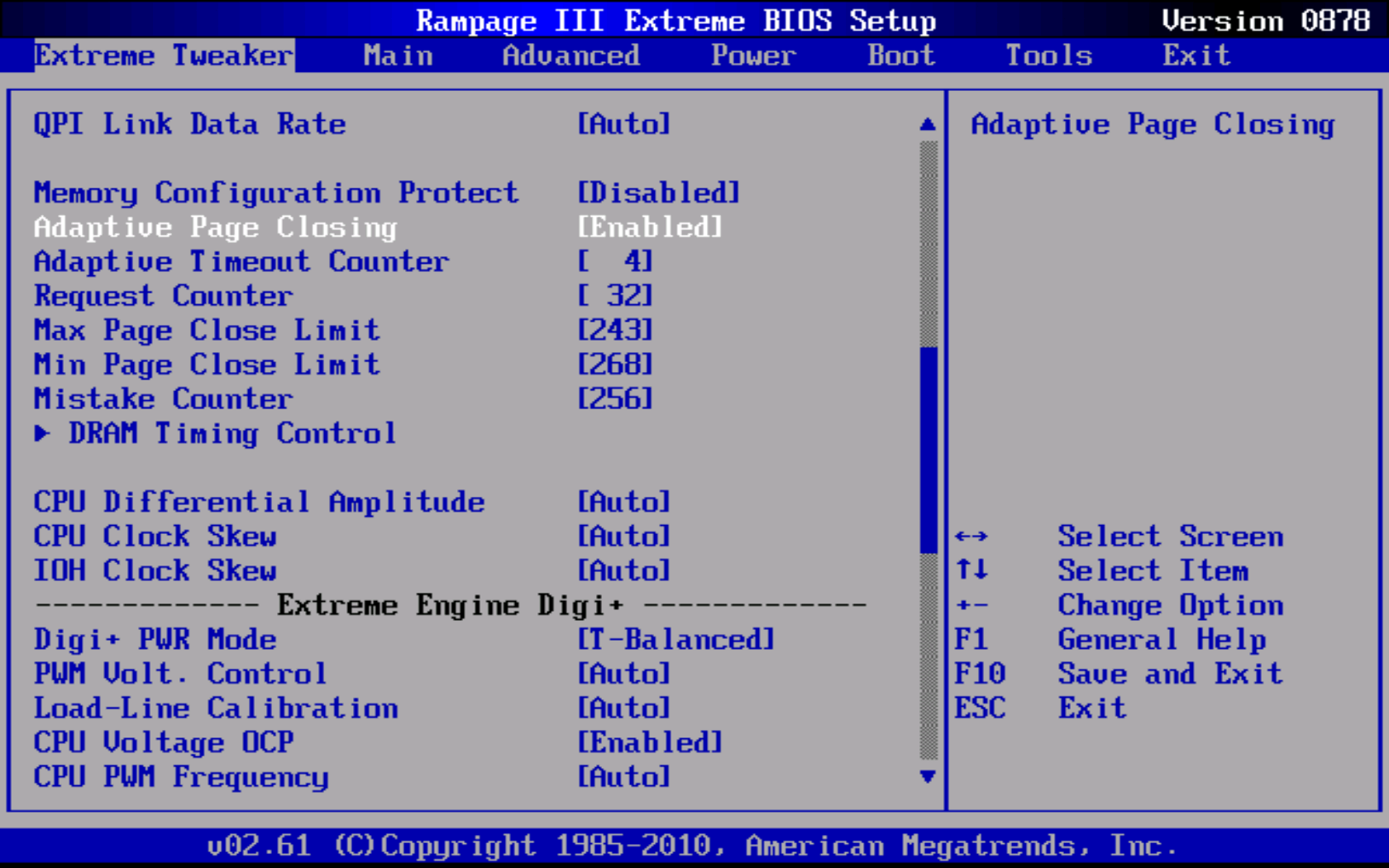
Here at AnandTech we decided to go the extra mile for you, our loyal reader. A few weeks back we approached ASUS USA Tech Support with a request to set-up a technical consultation with their Firmware Engineering Department. After passing along our request, what came out of the meeting was a special beta BIOS that added a number of previously unavailable memory tuning registers once excluded from direct user control.
In the interest of full disclosure, we did request the same help from EVGA and although they were willing to back our play, technical difficulties prevented them from delivering everything we had originally hoped for.
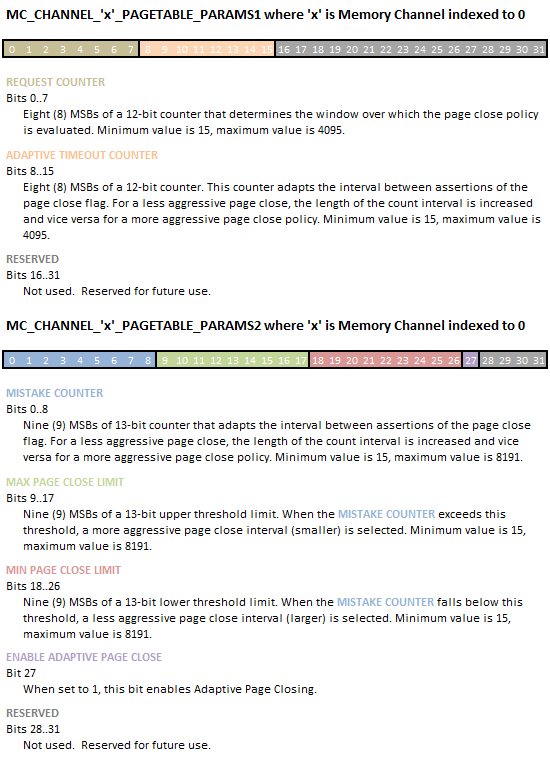
Seen below, these new registers are: Adaptive Page Closing, Adaptive Timeout Counter, Request Counter, Max Page Close Limit, Min Page Close Limit, and Mistake Counter. As suspected, the first setting is used to enabled or disable the feature entirely. Interesting enough, Intel chose not to enable this feature by default; so we leave it up to you.
Click to enlarge
A short description of each register is shown below (taken from Intel Core i7-900 Desktop Processor Extreme Edition Series and Intel Core i7-900 Desktop Processor Series Datasheet, Volume 2, page 79, dated October 2009). Be aware the source most likely contains at least one known error. In particular, Intel has provided exactly the same description for Adaptive Timeout Counter and Mistake Counter. As well, the bit count for Mistake Counter in the table does not match the value in the text, further suggesting someone goofed.
Once you've had time to fully digest the information above - and ponder how awesome we are - we would like to cordially invite you to do some of your own testing and report your results at our forums. AnandTech readers with a valid login can download ASUS Rampage III Extreme BIOS release 0878 now. We haven't really had a chance to do any significant experimenting with what little spare time we have and we need your help exploring uncharted territory...
We hope you’ve enjoyed reading this article as much as we’ve enjoyed putting it together. If you took the time to thoroughly peruse and digest the information within the intricacies of basic memory operation should no longer be such a baffling subject. With the ground work out of the way, we now have a solid platform from which to build as we more closely begin exploring other avenues for increasing memory performance. We’ve already identified additional topics worth discussing, and provided the time shows up on the books, plan to bring you more.
Assumedly, the one big question that may remain: What are the real world benefits of memory tuning? Technically, we covered the subject in-depth last year in a previous article. We suggest you read through it once again for a refresher before you embark on any overclocking journeys (or before you rush out to over-spend on memory kits). Everything written in that article then is just as valid today. We’ve run tests here on our Gulftown samples and found exactly the same behavior. Undoubtably, Intel have taken steps to ensure their architectures aren't prematurely bottlenecked by giving the memory controller a big, fat bus for communicating with the DIMMs.
From what we can tell, the next generation of performance processors from Intel are going to move over to a 256-bit wide (quad channel) memory controller, leaving little need for ultra-high frequency memory kits. Thus we re-iterate something many have said before: a top priority when it comes to improving memory ICs and their respective architectures should be to focus development on reducing absolute minimum latency requirements for timings such as CAS and tRCD, rather than chasing raw synthetic bandwidth figures or setting outright frequency records at the expense of unduly high random access times.
Stepping away from the performance segment for a moment, something else that's also come to light is rumored news that Intel's Sandy Bridge architecture (due Q1 2011) will, by design, limit reference clock driven overclocking on mainstream parts to 5% past stock operating frequency. If this is indeed the case the consequence will be a very restricted ability to control memory bus frequency with limited granularity to tune the first 50~70 MHz past each step, followed by mandatory minimum jump of 200MHz to the next operating level. Accessing hidden potential will be even more difficult, especially for users of mainstream memory kits. While there is no downside to this from a processing perspective (hey, more speed is always better), this could be another serious nail in the coffin of an already waning overclocking memory industry.